Bestand:Wafer flats convention v2.svg

Oorspronkelijk bestand (SVG-bestand, nominaal 150 × 150 pixels, bestandsgrootte: 13 kB)
| Dit is een bestand van Wikimedia Commons. Onderstaande beschrijving komt van de beschrijving van het bestand daar. |
Beschrijving
| Beschrijving |
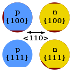
Wafer flats convention, based on Image:Wafer flats convention.PNG Conventional meaning of flats in semiconductor wafers. Red denotes material that has been removed. Wafer orientation is the orientation of the crystallographic plane in which the crystal grew. Wafer type indicated the type of doping.
|
| Datum | |
| Bron |
self-made, Deze niet W3C-verklaarde vectorafbeelding is gemaakt met Inkscape . |
| Auteur | Twisp |
| Andere versies | Wafer flats convention.PNG |
Licentie
| Ik, de auteursrechthebbende van dit werk, geef dit werk vrij in het publieke domein. Dit is wereldwijd van toepassing. In sommige landen is dit wettelijk niet mogelijk; in die gevallen geldt: Ik sta iedereen toe dit werk voor eender welk doel te gebruiken, zonder enige voorwaarden, tenzij zulke voorwaarden door de wet worden voorgeschreven. |
Bestandsgeschiedenis
Klik op een datum/tijd om het bestand te zien zoals het destijds was.
| Datum/tijd | Miniatuur | Afmetingen | Gebruiker | Opmerking | |
|---|---|---|---|---|---|
| huidige versie | 24 sep 2013 23:40 | | 150 × 150 (13 kB) | Cepheiden | fixed position of secondary flat Silicon processing for the VLSI era - Vol. 1 - Process technology; S Wolf; RN Tauber - Lattice Press; 1986; ISBN 096167237; p. 23 |
| 23 dec 2008 02:37 |  | 150 × 150 (13 kB) | Inductiveload | Added arrow indication <110> direction and enlarged flats so they can be easily seen | |
| 29 feb 2008 23:17 |  | 150 × 150 (9 kB) | Twisp | ||
| 29 feb 2008 23:13 |  | 150 × 150 (9 kB) | Twisp | ||
| 29 feb 2008 23:06 |  | 150 × 150 (8 kB) | Twisp | ||
| 29 feb 2008 22:59 |  | 150 × 150 (8 kB) | Twisp | ||
| 29 feb 2008 20:09 |  | 150 × 150 (9 kB) | Twisp | {{Information |Description= Wafer flats convention, based on Image:Wafer flats convention.PNG Conventional meaning of ''flats'' in semiconductor wafers. Black denotes material that has been removed. Wafer orientation is |
Bestandsgebruik
Dit bestand wordt op de volgende pagina gebruikt:
Globaal bestandsgebruik
De volgende andere wiki's gebruiken dit bestand:
- Gebruikt op ca.wikipedia.org
- Gebruikt op cs.wikipedia.org
- Gebruikt op de.wikipedia.org
- Gebruikt op en.wikipedia.org
- Gebruikt op es.wikipedia.org
- Gebruikt op et.wikipedia.org
- Gebruikt op eu.wikipedia.org
- Gebruikt op fi.wikipedia.org
- Gebruikt op it.wikipedia.org
- Gebruikt op it.wikibooks.org
- Gebruikt op ja.wikipedia.org
- Gebruikt op ko.wikipedia.org
- Gebruikt op pl.wikipedia.org
- Gebruikt op ro.wikipedia.org
- Gebruikt op sk.wikipedia.org
- Gebruikt op uk.wikipedia.org
- Gebruikt op www.wikidata.org